

Silicon Laboratory
The ETP Silicon Laboratory houses several measurement setups for the characterization of semiconductor structures specifically with regard to the effects of radiation damage like those suffered by the components in a collision experiment such as CMS:
- Probe stations for the general characterization of semicunductor structures such as diodes, MOS structures, strip sensors. The stations offer space for structures up to a size of 8" wafers. The sample temperature is controlled in the range of -20°C (CMS operating temperature and current reduction after irradiation) to +60°C (annealing studies). [IEKP-KA/2009-27]
- A sensitive IR camera is used to detect electroluminescence light.
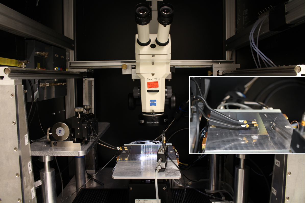
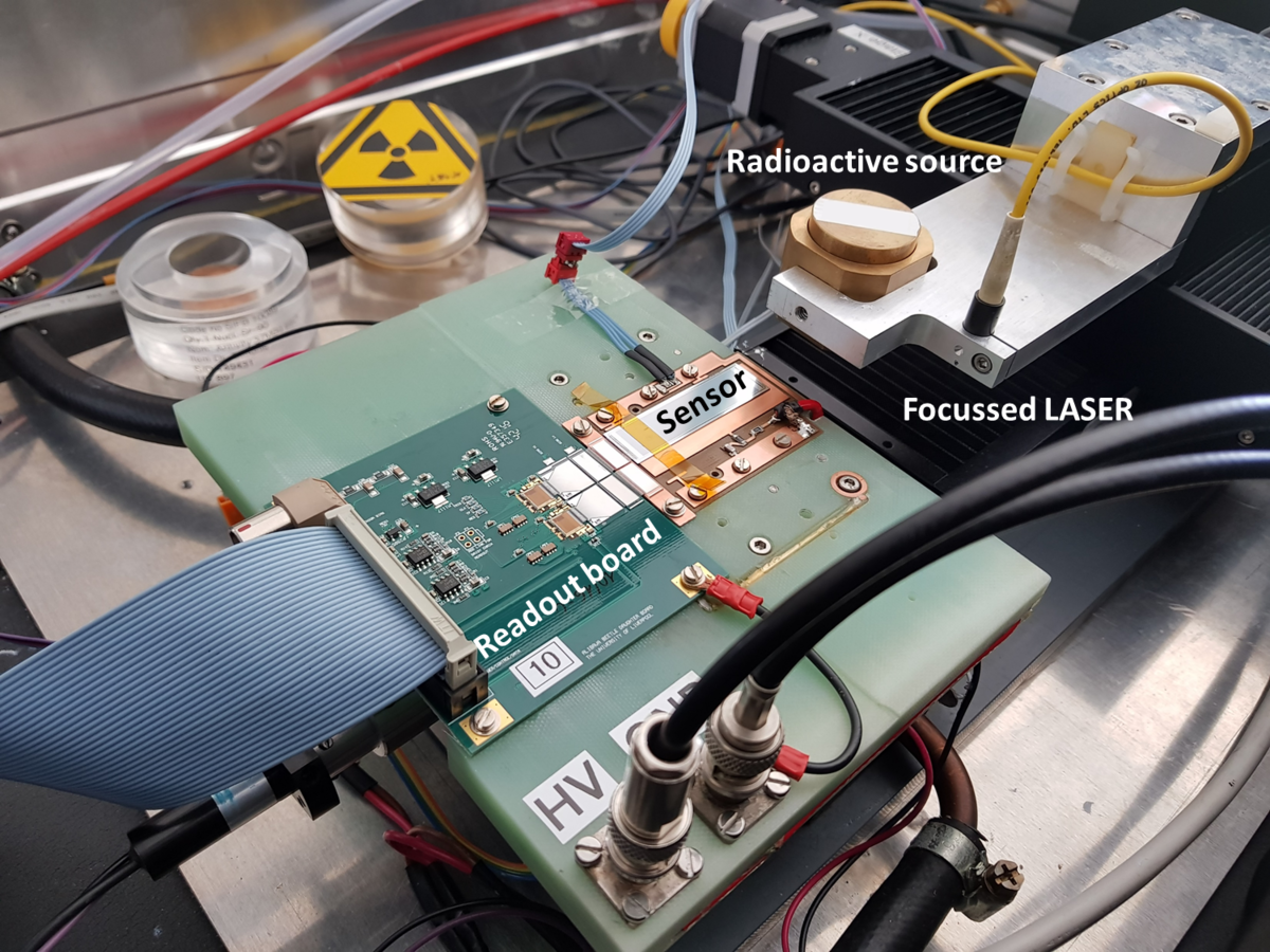
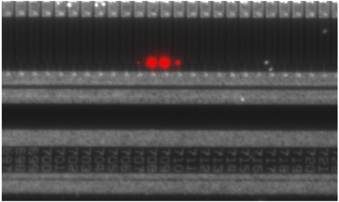
- Readout systems for strip sensors based on the ALiBaVa system. Here, too, the built-in sensors can be cooled or heated. A movable, focused IR laser and a Sr90 source are available for generating charge carriers. [IEKP-KA/2012-21]
In addition, we also operte readout systems with the new binary readout chip of the CMS track detector (CDC). [ETP-KA/2018-17]
The measurements are complemented by simulations with T-CAD Device Simulation Software. We use both Synopsys Sentaurus and Silvaco ATLAS. [IEKP-KA/2013-27]